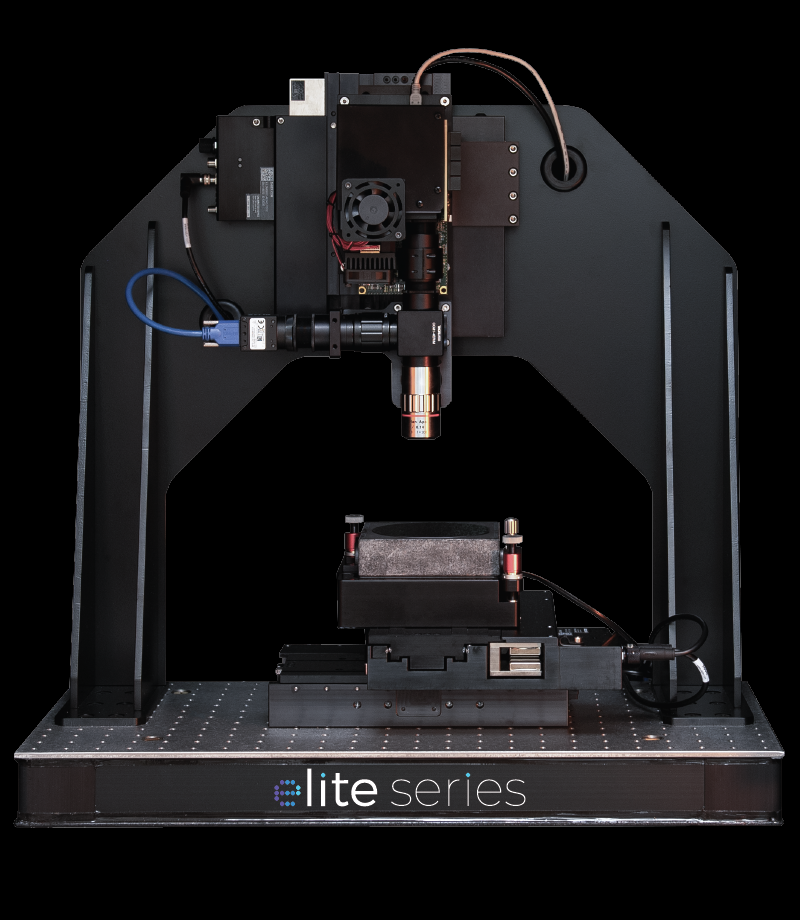
TERA-Fab® Elite series
Large-area maskless photolithography.
Key Features
Precise Multiwavelength Optics
Powered by the same advanced light engine as our E series 2.0, the Elite delivers high powered light with unparalleled uniformity across the projection area at the wavelength you need. Customize your Elite by choosing from a range of LED options that span from UV to visible wavelengths.

Single micron resolution over large areas
Our advanced DLP projection optics allow individual mirror projections down to (>1.25 µm) over areas up to mm2 in a single print by simply uploading a digital mask design to our Elite OS software. The Elite features a vacuum chuck sample holder that can handle samples up to 4” in diameter.

An Intelligent Digital Photomask Platform
Take advantage of our maskless pattern design platform and gain the ability to conduct truly arbitrary nano-and-micropatterning over mm2 to cm2 areas. By simply uploading an image (PNG, JPG, BMP), users can change their pattern design on the fly.

Automating Your Experience
Automating critical setup steps such as stage leveling and identifying the focal plane reduces human error and increases print quality. The Elite instrument features numerous automated functionalities that not only increase precision but provide a more enjoyable user experience.

Control With Simplicity
Simple and intuitive hardware and software design allows users of any background to rapidly prototype with Elite after only a few hours of training. The eliteOS software provides full control over key patterning parameters that can be tailored for any application.

Team TERA, At Your Service
We take pride in our ability to serve our global user base with both on-site and virtual support. Team TERA is actively engaging with customers to ensure the best possible user experience.

Applications

Microfluidic Devices
Rapidly prototype microfluidic channel molds using conventional positive or negative photoresists right from your desktop.

Bioengineering
Generate complex hydrogel scaffolds via extracellular matrix (ECM) photopolymerization to create in vitro platforms with sub-cellular resolution.

Grayscale Lithography
Pattern complex features with 8-bit depth using dynamic exposure and reduced light intensity.
And many more.
Technical Specifications
| Servo X-Y scan range (closed loop) | 110 mm x 110 mm |
| Servo Z scan range (closed-loop) | 60 mm |
| Repeatability | <0.08μm |
| Unidirectional accuracy | 1μm |
| Travel Speeds | 0-1,200μm/s |
| ΘX and ΘY 2-axis angular positioning | ±12600 arcseconds angular range, 0.144 arcseconds angular resolution |
| Motorized Z positioning | 60 mm travel range, Unidirectional accuracy: 1 μm, maximum speed: 1,200 mm/s |
| Digital Light Processing (DLP) | DLP5500 1024 x 768 resolution |
| Light Sources | UV LED Light Engine (405 nm) 2.4-2.8 W, Green LED Light Engine (532 nm) 2.5 W, additional 460 nm and 365 nm options available |
| 5x and 20x Objective Lenses (Exchangeable) | 34 mm working distance, 2 μm resolving power |
| Field of View | 1.48 mm x 1.11 mm (with 5x objective installed) |
| CMOS camera | 12 MP (4000 x 3000), 0.74 cm x 0.56 cm sensor size, 1.85 μm x 1.85 μm pixel size |
| X-Y long travel stage motors |
|
|
| Z positioning of sample stage |
|
|
|
| Patterning |
|
|
|
| Optics |
|
|
|